| Issue |
Renew. Energy Environ. Sustain.
Volume 2, 2017
Sustainable energy systems for the future
|
|
|---|---|---|
| Article Number | 7 | |
| Number of page(s) | 5 | |
| DOI | https://doi.org/10.1051/rees/2017019 | |
| Published online | 24 August 2017 | |
Research Article
Perovskite solar cells for roll-to-roll fabrication
School of Photovoltaics and Renewable Energy Engineering, University of New South Wales,
Sydney
2052, Australia
* e-mail: This email address is being protected from spambots. You need JavaScript enabled to view it.
Received:
5
January
2017
Received in final form:
23
June
2017
Accepted:
27
July
2017
Abstract
Perovskite solar cell (PSCs) is considered as the game changer in emerging photovoltaics technology. The highest certified efficiency is 22% with high temperature processed (∼500 °C) TiO2 based electron transport layer (ETL). High temperature process is a rudimentary hindrance towards roll-to-roll processing of PSCs on flexible substrates. Low temperature solution process (<150 °C) ZnO based ETL is one of the most promising candidate for large scale roll-to-roll fabrication of cells as it has nearly identical electron affinity (4.2 eV) of TiO2. The mixed organic perovskite (MA0.6FA0.4PbI3) devices with Al doped ZnO (AZO) ETL demonstrate average cell efficiency over 16%, which is the highest ever reported efficiency for this device configuration. The energy level alignment and related interfacial charge transport dynamics at the interface of ZnO and perovskite films and the adjacent charge transport layers are investigated. Significantly improved device stability, hysteresis free device photocurrent have been observed in MA0.6FA0.4PbI3 cells. A systematic electrochemical impedance spectroscopy, frequency dependent capacitance spectra, surface morphology and topography characterization have been conducted to understand the role of interfacial electronic properties between perovskite and neighbouring layers in perovskite device. A standardized degradation study, interfacial electronic property and capacitive spectra analysis of aged device, have been measured to understand the enhanced device stability in mixed MA0.6FA0.4PbI3 cells. Slow perovskite material decomposition rate and augmented device lifetime with AZO based devices have been found to be correlated with the more hydrophobic and acidic nature of AZO surface compared to pristine ZnO film.
© A. Uddin et al., published by EDP Sciences, 2017
 This is an Open Access article distributed under the terms of the Creative Commons Attribution License (http://creativecommons.org/licenses/by/4.0), which permits unrestricted use, distribution, and reproduction in any medium, provided the original work is properly cited.
1 Introduction
Organic–inorganic hybrid solar cells using metal-halide perovskites such as methylammonium lead iodide (CH3NH3PbI3) as light harvesters exhibit several appealing features such as high optical cross section, excellent ambipolar charge transport, small exciton binding energy, tunable band gaps, and low-cost fabrication [1]. Importantly, the CH3NH3PbI3 perovskite solar cells (PSCs) are solution-processable, which is beneficial to inexpensive largescale commercialization. Over the past few years several groups have reported high power conversion efficiencies (PCEs) up to 22% raising expectations for PSCs to be deployed on a large scale along with conventional silicon based solar cells [2]. The highest efficient cells 22% was fabricated with high temperature processed (∼500 °C) TiO2 based electron transport layer (ETL). It is very important to develop a low temperature process technology (<150 °C) for the roll-to-roll fabrication of perovskite cell on flexible substrate.
Zinc oxide (ZnO) is known to have an electron mobility that is substantially higher than that of TiO2, which makes it an ideal choice for an electron-selective contact. The ZnO nanoparticle layer can be deposited easily by spin coating and requires no heating or sintering step, which makes it ideal for deposition on thermally sensitive substrates. The solution-processing of the ZnO layer is simple, economical and proceeds at room temperature, which gives it important advantages over other cell designs that use mesoporous scaffolds or vapour-phase deposition techniques [3]. The thickness of ZnO film can be varied systematically by repeating the spin-coating process several times. However, alkaline ZnO surface helps to produce methyl ammonium ion (CH3NH3+) when the perovskite film grown on ZnO and annealed at temperature around 100 °C [4]. The perovskite crystal structure on ZnO ETL undergoes thermal decomposition even at temperature 100 °C annealing. This thermal instability of perovskite film on ZnO ETL is a major bottleneck towards practical application of PSC under sunlight.
The chemical formula of mixed organic cation PSCs can be expressed as: ABX3, where A stands for a combination of methyl ammonium (MA) [CH3NH3+] and formamidinium (FA) [HN=CHNH3+] organic cations, B denotes a divalent metal ion (usually Pb or Sn) and X symbolizes individual halogen element (I or Br or Cl). The high ionic radius (1.9–2.2 Å) of the formamidinium cation is bigger than that of methyl ammonium ion (1.8 Å) [5]. The formamidinium based perovskite material has a higher perovskite tolerance factor because of their bigger ionic radius which provides much better structural stability [6]. However, the open circuit voltage (VOC) is relatively low in such a pristine formamidinium perovskite device resulting in a relatively lower device performance compared to that with methyl ammonium lead triiodide perovskite based PSCs [7]. The optimum trade-off between extended absorption and suppressed VOC, the concept of mixed organic cation based perovskite has come into effect which tunes the perovskite bandgap by incorporating both the methylammonium and formamidinium organic cations in a single ABX3 crystal structure [8].
Here we have demonstrated significance is achieved in mixed organic cation based planar perovskite (MA0.6FA0.4PbI3) devices with low temperature (<150 °C) solution processed AZO thin films as ETL using sol–gel technique. The fabricated perovskite device exhibited high PCE of over 16% and device stability >570 h. Present work is also to demonstrate the in-depth analysis into the charge transfer characteristics at the interface between mixed organic cation perovskite layer and adjacent charge selective interlayer (AZO). An elaborate surface morphology and surface topography measurements are also carried out to probe into the superior performance/stability of the AZO based devices. A month-long, systematic degradation study was performed to confirm the superior lifetime of MA0.6FA0.4PbI3/AZO based devices corroborated by the extensive analysis of electronic parameters like interfacial contact resistance, recombination resistance, flat-band potential and low frequency regime interfacial capacitance (electrode polarization) of both the fresh and aged devices.
2 Methodology
Patterned ITO/glass substrates were washed with Hellmanex III soap, DI water, acetone and isopropanol with duration of 10 min each. For ZnO ETL, 0.48 M sol–gel ZnO precursor solution was prepared by dissolving zinc acetate dehydrate (Zn(CH3COO)2·2H2O, Sigma-Aldrich, >99.0%) in 2-methoxyethanol (CH3OCH2CH2OH, Sigma-Aldrich, 99.8%, anhydrous) with an additive ethanolamine (NH2CH2CH2OH, Sigma-Aldrich, >99.5%) by stirring for 24 h. For AZO ETL, a 0.05 M aluminum nitrate nonahydrate (Al(NO3)3·9H2O, Sigma-Aldrich) solution in 2-methoxyethanol was prepared and stirred for 1 h at 80 °C. A 15 wt% AZO precursor solution was prepared by mixing the as prepared aluminum nitrate nonahydrate solution with sol–gel ZnO precursor solution in required weight ratio. Both the sol–gel ZnO and AZO precursor solutions were spin coated on ITO/glass substrate at 4000 rpm for 60 s and then annealed on a hotplate at 140 °C for half an hour. 1 M PbI2 solution in DMF (N,N-dimethylformamide, Sigma-Aldrich, anhydrous) with 120 mL 4-TBP (4-tert-butylpyridine, Sigma-Aldrich) was prepared at a temperature of 70 °C. The PbI2 solution was spin cast on ZnO/AZO coated substrate at 3000 rpm for 30 s. Before spin coating, both the substrates and the solution were kept at 70 °C. Then the substrates were annealed at 100 °C for 1 h and then dipped in a 2-propanol solution having a total iodide concentration of 0.0628 M with the mole fraction of CH3NH3I (MAI) and HN=CHNH3I (FAI) to be 0.6 and 0.4, respectively. The devices were annealed for 10 min at 75 °C after the dipping. For HTL, 73.3 mg mL−1 Spiro-OMeTAD (2,20,7,70-tetrakis (N,N-di-p-methoxyphenylamino)-9,90-spirobiftuorene, sublimed grade 99.8%, Borun chemicals) in chlorobenzene was doped with 17.5 mL Li-TFSI (520 mg mL−1 in acetonitrile) and 28.8 mL 4-TBP. The Spiro-OMeTAD layer was spin coated on the perovskite layer with 1200 rpm for 30 s. Finally, 100 nm Ag layer was deposited on the Spiro-OMeTAD HTL coated substrate by thermal evaporation with an evaporation rate of 2 Å s−1 under a vacuum condition of 1 × 10⁻⁶ mbar. The device area was flexed to be 0.045 cm2 with the use of a metal mask. So, the overall device structures were: ITO/sol–gel ZnO or AZO/MA0.6FA0.4PbI3 perovskite/Spiro-OMeTAD/Ag.
The current−voltage characteristics of the devices were measured with a NREL calibrated Keithley 2400 Source Meter under 100 mW cm−2 (AM 1.5G) simulated sunlight. For optical characterization like transmittance, reflectance and absorbance measurement, a UV–VIS-NIR spectrometer (Perkin Elmer − Lambda 950) was used. X-ray diffraction (XRD) with CuKα radiation was performed by step-scanning with a step size of 0.02°. Surface topology and device cross sectional view were captured by Carl Zeiss AURIGA Cross Beam SEM (scanning electron microscopy) and the surface roughness was measured with Bruker Dimension ICON SPM AFM (atomic force microscopy) machine. The impedance analysis was conducted with an Autolab PGSTAT-30 equipped with a frequency analyzer module in the frequency range from 1 MHz to 10 Hz. AC oscillating amplitude was as low as 20 mV (RMS) to maintain the linearity of the response. External quantum efficiency measurements were performed using a QEX10 spectral response system from PV Measurements Inc.
3 Results
The MA0.6FA0.4PbI3 perovskite film was deposited on top of both ZnO and AZO films in an identical way using two step dipping method. It was confirmed from the XRD pattern of MA0.6FA0.4PbI3 perovskite film that the formations of mixed organic cation perovskite in which both MAI and FAI organic cations have been incorporated in the same lattice frame [9]. The optical properties MA0.6FA0.4PbI3/ZnO and MA0.6FA0.4PbI3/AZO films on top of ITO/glass substrates were investigated with absorbance measurement. The absorbance pattern of MA0.6FA0.4PbI3/ZnO and MA0.6FA0.4PbI3/AZO films showed the onset for both the films 820 nm which is similar with the red-shifted spectral response achieved with mixed organic cation perovskite (MA0.6FA0.4PbI3) compared to mono organic methyl ammonium lead triiodide perovskite (MAPbI3), having an absorption onset around ∼800 nm [10].
Figure 1A and B illustrates the SEM surface morphology image of MA0.6FA0.4PbI3/ZnO and MA0.6FA0.4PbI3/AZO films, respectively, on ITO/glass substrate. As observed from Figure 1 the grain size of MA0.6FA0.4PbI3 perovskite grown on AZO ETL film is larger compared to that grown on ZnO ETL film. The variation in the surface morphology of identically fabricated perovskite film on different ETL films is similar with the earlier findings that the formation of perovskite film can be significantly modified based on the underlying layer.
The fabricated solar cells performance of MA0.6FA0.4PbI3 perovskite absorber with low temperature processed ZnO and AZO ETLs have been measured. We have investigated the device performance of MA0.6FA0.4PbI3 perovskite with pristine ZnO and different Al concentration of AZO as ETL. The best performing MA0.6FA0.4PbI3/AZO device exhibits a PCE of 16% with the JSC, VOC and FF value being 20.2 mA cm−2, 1014.160 mV and 71%, respectively. Figure 2 shows the J–V curves of the best performing MA0.6FA0.4PbI3/ZnO and MA0.6FA0.4PbI3/AZO devices, respectively. The high reproducibility of both the device structures is evident from the statistical histograms (with normal distribution) of PCE, JSC, VOC and FF of 10 identically fabricated MA0.6FA0.4PbI3/ZnO and MA0.6FA0.4PbI3/AZO devices.
The average values of JSC, VOC and FF for these devices are 20.18 mA cm−2, 1004.46 mV and 68.89%, respectively. To the best of our knowledge, the average PCE 14.9% reported in our study is the highest ever average PCE attained with MA0.6FA0.4PbI3 perovskite device processing at low temperature processed AZO layer. The MA0.6FA0.4PbI3/ZnO devices demonstrate comparatively lower average PCE of 11.82% with the average JSC, VOC and FF values being 21.44 mA cm−2, 973.48 mV and 56.69%, respectively. Even the best performing MA0.6FA0.4PbI3/ZnO device shows relatively degraded photovoltaic performance (PCE: 13.40%, JSC: 22.39 mA cm−2, VOC: 984.24 mV and FF: 60.66%) in contrast with the average performance exhibited by MA0.6FA0.4PbI3/AZO devices.
Our un-encapsulated MA0.6FA0.4PbI3/ZnO and MA0.6FA0.4PbI3/AZO samples were stored for 30 days in a N2 filled glovebox following the protocols mentioned in earlier perovskite degradation studies under dark and device performance was evaluated at regular intervals at humidity controlled (35–40% relative humidity) ambience at room temperature. We measured the J–V curves of MA0.6FA0.4PbI3/ZnO and MA0.6FA0.4PbI3/AZO devices, respectively, throughout the time period of degradation study (30 days) with certain intervals as shown in Figure 3. The highest PCE for AZO or ZnO ETL based devices can be obtained after 4–5 days, which is consistent with the identical trend reported in previous perovskite literatures [11].
To understand the reasons behind the device stability with MA0.6FA0.4PbI3/AZO devices, we have conducted impedance characterization of 30 day-aged MA0.6FA0.4PbI3/ZnO and MA0.6FA0.4PbI3/AZO devices. The fitted values of various electronic parameters using equivalent circuit model we have estimated the contact resistance for both samples. Since, the HTL layer (Spiro-OMeTAD in both cases) remains constant for both the device structures, the variation in device contact resistance can be attributed to the disparity in degradation phenomena of the ETL layers (ZnO and AZO) and their concomitant influence on the decomposition of neighbouring MA0.6FA0.4PbI3 perovskite film.
Reduced interface trapping phenomena in MA0.6FA0.4PbI3/AZO devices can be attributed to the reduced perovskite grain boundary aided by large grain atop AZO film and trap state filling in AZO associated with Burstein–Moss effect [12]. Subdued interfacial trapping endows with suppressed recombination phenomenon in aged MA0.6FA0.4PbI3/AZO devices which is also congruent with 95% higher recombination resistance compared to MA0.6FA0.4PbI3/ZnO devices as shown in Figure 4. The higher recombination and shunt resistance in aged MA0.6FA0.4PbI3/AZO devices contribute to their higher VOC value which leads to enhanced device stability in contrast with MA0.6FA0.4PbI3/ZnO devices.
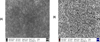 |
Fig. 1 Surface morphology view (SEM image) of MA0.6FA0.4PbI3 perovskite film on top of (A) ZnO and (B) Al doped ZnO (AZO) film. |
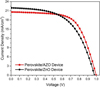 |
Fig. 2 J–V characteristics of MA0.6FA0.4PbI3 perovskite/ZnO and MA0.6FA0.4PbI3 perovskite/AZO devices at room temperature. |
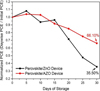 |
Fig. 3 30 Days normalized PCE of MA0.6FA0.4PbI3/ZnO and MA0.6FA0.4PbI3/AZO devices attained from a systematic stability study. MA0.6FA0.4PbI3/AZO devices retain higher normalized PCE compared to MA0.6FA0.4PbI3/ZnO devices. |
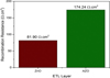 |
Fig. 4 Recombination resistance (fitted data from impedance spectroscopy at 0.9 V under dark) of MA0.6FA0.4PbI3 perovskite devices containing ZnO and AZO (Al doped ZnO) ETL. |
4 Discussion
Boyen et al. [13] has reported that the interparticle connectivity of perovskite grain and its surface morphology can be enhanced by the removal of residual impurities from the underneath metal oxide ETL. It has already been reported that the residual impurities like hydroxyl (OH−) ions and organic CH3COO− radicals are significantly reduced in Al dopant incorporated ZnO film compared to pristine ZnO film. The larger grain size of MA0.6FA0.4PbI3 perovskite grown on AZO ETL film can be attributed to the enhanced interparticle connectivity of perovskite owing to the significantly reduced residual impurity [14] at the underneath AZO film. From the statistical quantity analysis of AFM images, the RMS surface roughness of MA0.6FA0.4PbI3/AZO film (55.7 nm) has been found to be lower than that (56.80 nm) of MA0.6FA0.4PbI3/ZnO film [9].
The initial rise in PCE of devices in Figure 3 can be attributed to the substantial rise in FF value which is related to the oxidation of Spiro-OMeTAD HTL in ambient condition for improved hole conductivity and thus more efficient charge extraction. As comprehended from Figure 3, MA0.6FA0.4PbI3/AZO devices retain nearly 70% of their initial PCE even after 1 month, whereas for MA0.6FA0.4PbI3/ZnO, PCE drops down to 36% of the commencing PCE during the same time range which denotes nearly two times higher stability with MA0.6FA0.4PbI3/AZO devices. As observed in Figure 3, about two-fold enhancement in device stability with MA0.6FA0.4PbI3/AZO devices originates from two times higher JSC and about 8% higher VOC values retained in MA0.6FA0.4PbI3/AZO devices compared to MA0.6FA0.4PbI3/ZnO in course of 1 month long degradation study. In general, perovskite film decomposes rapidly in the presence of water vapour [15]. Since, ZnO film is hygroscopic, it traps water at its surface [16] and with aging, ZnO becomes saturated with moisture. Due to the more hydrophobic nature of AZO film, the trapped moisture-assisted perovskite decomposition rate is expected to be lower in MA0.6FA0.4PbI3/AZO devices, which explicates higher JSC and lower contact resistance retained in the MA0.6FA0.4PbI3/AZO devices which eventually lead to their higher stability compared to MA0.6FA0.4PbI3/ZnO devices. In an aged perovskite device, small voids present in Spiro-OMeTAD HTL film trigger the migration of CH3NH3I ion through them to react with silver cathode and produce AgI (silver iodide) which results in the decomposition in perovskite layer [17].
The large grain size and concomitant reduction in MA0.6FA0.4PbI3 perovskite grain boundary overlying the AZO layer ensure superior charge transfer across the interface thereby lowering the donor–acceptor pair recombination and significantly suppressing current leakage phenomena, which correlate to their efficient charge extraction and enhanced fill factor. The enhanced flat-band potential coupled with high recombination resistance from impedance measurement explains the larger open circuit voltage observed in MA0.6FA0.4PbI3/AZO devices and its implication on high PCE [9].
In summary, we have reported a highly efficient (∼16%) mixed organic cation based pure triiodide (MA0.6FA0.4PbI3) perovskite device fabricated with a low temperature processed AZO ETL in a planar device structure. The present work demonstrates simultaneous enhancement in device performance and stability in PSCs fortified with low hysteresis and opens up a new research pathway towards the fabrication of less energy extensive, flexible substrate compatible, efficient PSCs exhibiting superior device performance, stability and reduced photocurrent hysteresis behaviour for reliable operation aimed at long term practical applications.
Acknowledgments
The authors gratefully acknowledge the financial support provided by Future Solar Technologies Pty. Ltd. for this research work. The authors would also like to acknowledge the endless support from the staffs of Photovoltaic and Renewable Energy Engineering School, Electron Microscope Unit (EMU) and Solid State and Elemental Analysis Unit under Mark Wainwright Analytical Centre, UNSW.
References
- P.-W. Liang, C.-Y. Liao, C.-C. Chueh, F. Zuo, S.T. Williams, X.-K. Xin, J. Lin, A.K.Y. Jen, Adv. Mater. 26, 3748 (2014) [CrossRef] [Google Scholar]
- NREL, Photovoltaics efficiency chart, 2016, http://www.nrel.gov/ncpv/images/efficiency_chart.jpg [Google Scholar]
- Y. Zhou, M. Yang, W. Wu, A.L. Vasiliev, K. Zhu, N.P. Padture, J. Mater. Chem. A 3, 8178 (2015) [CrossRef] [Google Scholar]
- J. Yang, B.D. Siempelkamp, E. Mosconi, F. De Angelis, T.L. Kelly, Chem. Mater. 27, 4229 (2015) [CrossRef] [Google Scholar]
- N.J. Jeon, J.H. Noh, W.S. Yang, Y.C. Kim, S. Ryu, J. Seo, S.I. Seok, Nature 517, 476 (2015) [CrossRef] [Google Scholar]
- T.M. Koh, K. Fu, Y. Fang, S. Chen, T.C. Sum, N. Mathews, S.G. Mhaisalkar, P.P. Boix, T. Baikie, J. Phys. Chem. C 118, 16458 (2014) [CrossRef] [Google Scholar]
- S. Aharon, A. Dymshits, A. Rotem, L. Etgar, J. Mater. Chem. A 3, 9171 (2015) [CrossRef] [Google Scholar]
- N. Pellet, P. Gao, G. Gregori, T.-Y. Yang, M.K. Nazeeruddin, J. Maier, M. Grätzel, Angew. Chem. Int. Ed. 53, 3151 (2014) [CrossRef] [Google Scholar]
- M.A. Mahmud, N.K. Elumalai, M.B. Upama, D. Wang, M. Wright, T. Sun, C. Xu, F. Haque, A. Uddin, RSC Adv. 6, 86108 (2016) [CrossRef] [Google Scholar]
- D. Liu, T.L. Kelly, Nat. Photon. 8, 133 (2014) [CrossRef] [Google Scholar]
- J. You, L. Meng, T.-B. Song, T.-F. Guo, Y. Yang, W.-H. Chang, Z. Hong, H. Chen, H. Zhou, Q. Chen, Y. Liu, N. De Marco, Y. Yang, Nat. Nanotechnol. 11, 75 (2015) [CrossRef] [Google Scholar]
- A. Aprilia, P. Wulandari, V. Suendo, A. Herman, R. Hidayat, A. Fujii, M. Ozaki, Sol. Energy Mater. Sol. Cells 111, 181 (2013) [CrossRef] [Google Scholar]
- B. Conings, L. Baeten, T. Jacobs, R. Dera, J. D'Haen, J. Manca, H.-G. Boyen, APL Mater. 2, 81505 (2014) [CrossRef] [Google Scholar]
- T. Salim, S. Sun, Y. Abe, A. Krishna, A.C. Grimsdale, Y.M. Lam, J. Mater. Chem. A 3, 8943 (2015) [CrossRef] [Google Scholar]
- J. Yang, B.D. Siempelkamp, D. Liu, T.L. Kelly, ACS Nano 9, 1955 (2015) [CrossRef] [Google Scholar]
- Y. Sun, J.H. Seo, C.J. Takacs, J. Seifter, A.J. Heeger, Adv. Mater. 23, 1679 (2011) [Google Scholar]
- Y. Kato, L.K. Ono, M.V. Lee, S. Wang, S.R. Raga, Y. Qi, Adv. Mater. Interfaces 2, 1500195 (2015) [CrossRef] [Google Scholar]
![[Google Scholar]](https://scholar.google.com/scholar?q=NREL%2C+Photovoltaics+efficiency+chart%2C+2016%2C+www.nrel.gov%2Fncpv%2Fimages%2Fefficiency_chart.jpg)
Cite this article as: Ashraf Uddin, Md Arafat Mahmud, Naveen Kumar Elumalai, Dian Wang, Mushfika Baishakhi Upama, Matthew Wright, Kah Howe Chan, Faiazul Haque, Cheng Xu, Perovskite solar cells for roll-to-roll fabrication, Renew. Energy Environ. Sustain. 2, 7 (2017)
All Figures
|
Fig. 1 Surface morphology view (SEM image) of MA0.6FA0.4PbI3 perovskite film on top of (A) ZnO and (B) Al doped ZnO (AZO) film. |
| In the text | |
|
Fig. 2 J–V characteristics of MA0.6FA0.4PbI3 perovskite/ZnO and MA0.6FA0.4PbI3 perovskite/AZO devices at room temperature. |
| In the text | |
|
Fig. 3 30 Days normalized PCE of MA0.6FA0.4PbI3/ZnO and MA0.6FA0.4PbI3/AZO devices attained from a systematic stability study. MA0.6FA0.4PbI3/AZO devices retain higher normalized PCE compared to MA0.6FA0.4PbI3/ZnO devices. |
| In the text | |
|
Fig. 4 Recombination resistance (fitted data from impedance spectroscopy at 0.9 V under dark) of MA0.6FA0.4PbI3 perovskite devices containing ZnO and AZO (Al doped ZnO) ETL. |
| In the text | |
Current usage metrics show cumulative count of Article Views (full-text article views including HTML views, PDF and ePub downloads, according to the available data) and Abstracts Views on Vision4Press platform.
Data correspond to usage on the plateform after 2015. The current usage metrics is available 48-96 hours after online publication and is updated daily on week days.
Initial download of the metrics may take a while.